[ad_1]
This strategy preserves the fragile bodily properties of the 2D materials.
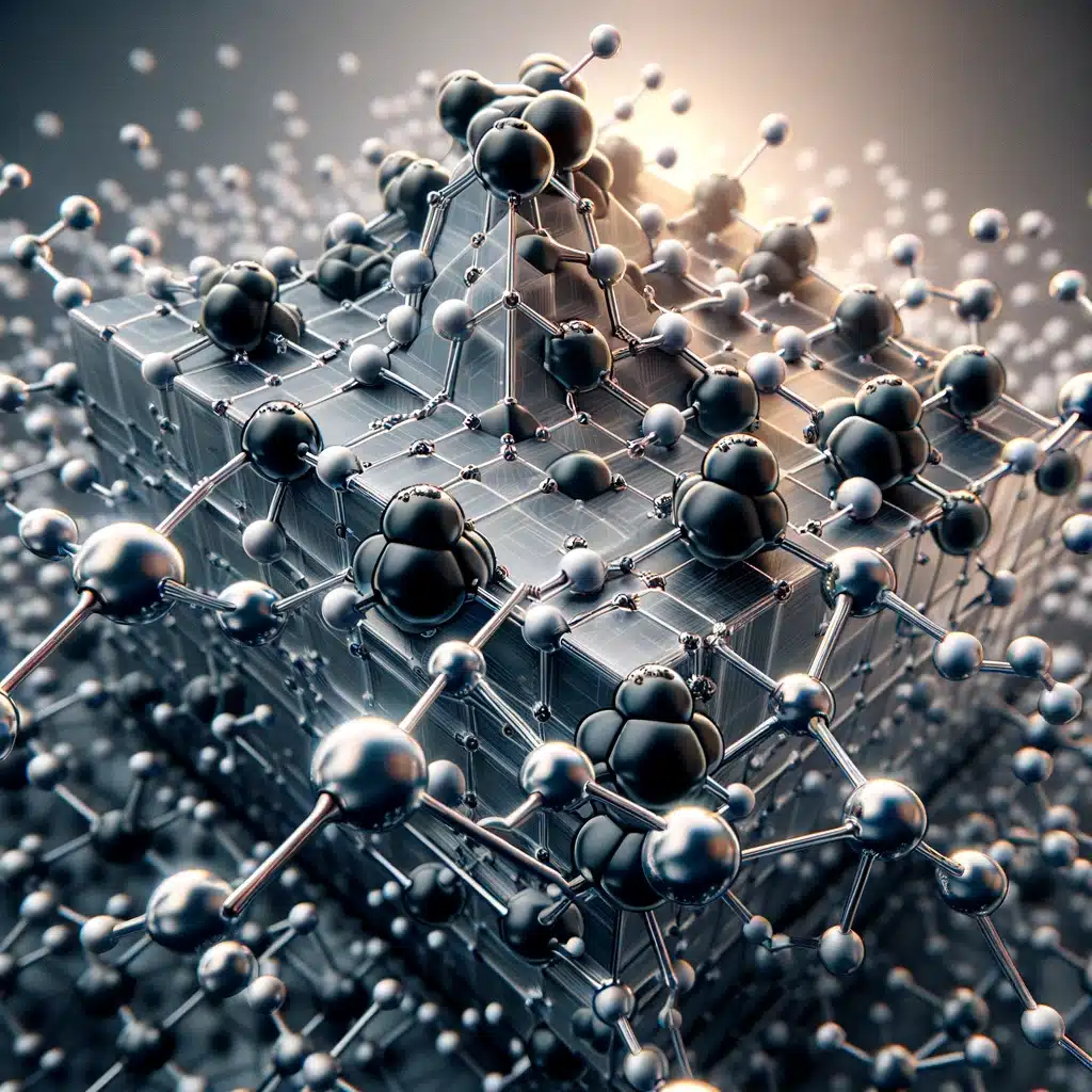
Researchers at Hunan College, the Chinese language Academy of Sciences and Wuhan College lately have developed a novel fabrication methodology for monolayer black phosphorus (BP) and germanium arsenide (GeAs) transistors utilizing a method based mostly on van der Waals peeling. This methodology represents a exceptional innovation within the dealing with and manipulation of 2D supplies.
The event of monolayer transistors utilizing two-dimensional (2D) semiconductors like black phosphorus and germanium arsenide marks a major breakthrough within the area of scaled digital units. The fabrication course of for these supplies, nevertheless, has confronted substantial challenges, primarily as a result of inherent difficulties in forming secure and sturdy electrical contacts with these fragile 2D supplies.
The van der Waals peeling method includes a layer-by-layer mechanical peeling course of. This methodology permits the channel area of a multilayer black phosphorus transistor to be step by step thinned all the way down to a monolayer. All this whereas sustaining the integrity of its delicate lattice construction and retaining a thicker, multilayer contact area. This strategy preserves the fragile bodily properties of the 2D materials, that are important for the optimum efficiency of the transistor.
An attention-grabbing remark from the utilisation of this method is the change within the electrical properties of the 2D transistor because the channel thickness varies. It was discovered that the provider mobility in black phosphorus decreases considerably when its physique thickness is decreased. This behaviour is extra akin to that of a traditional bulk semiconductor, relatively than a pure van der Waals semiconductor, which regularly displays completely different digital traits.
The flexibility to control and examine these supplies at such a tremendous scale opens up new avenues for analysis and growth in semiconductor expertise, probably resulting in extra environment friendly, smaller, and quicker digital units. Furthermore, the van der Waals peeling method may very well be a game-changer within the fabrication of 2D semiconductors, providing a extra managed and fewer invasive strategy to creating monolayer units.
[ad_2]