
[ad_1]
Using 3D interconnects in miniaturized photonic energy units, leads to a sixfold improve in wafer space utilization.
The College of Ottawa, collaborating with nationwide and worldwide companions, has efficiently manufactured the world’s first back-contact micrometric photovoltaic cells. Remarkably small, these cells are solely twice the thickness of a human hair. They provide appreciable benefits over conventional photo voltaic applied sciences, primarily by decreasing the shadowing attributable to electrodes by 95%. This innovation has the potential to considerably decrease the prices of vitality manufacturing, doubtlessly decreasing them by as much as thrice.
To advance chip miniaturization and improve energy density, a novel method to manufacture 3D interconnects on multijunction photo voltaic cells has been developed. This course of incorporates methods like III-V heterostructure plasma etching, gold electro-deposition, and chemical-mechanical sprucing, integrating through-substrate vias into the heterostructure.
Skinny III-V movies, as small as 20 micrometers, are managed by wafer bonding. This technique has efficiently produced photonic energy units which can be smaller by three orders of magnitude, in comparison with commonplace chips, whereas sustaining a minimal shading issue under 3%.
Using 3D interconnects, in distinction to conventional 2D connections in miniaturized photonic energy units, leads to a six-fold improve in wafer space utilization. These developments not solely enhance energy yield per wafer but in addition pave the best way for high-density, miniaturized units in purposes like energy over fiber, the web of issues, and micro-concentrator photovoltaics.
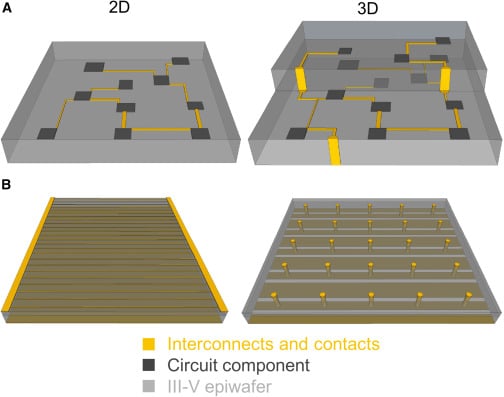
This research showcases a pioneering method to enhancing energy units by three-dimensional (3D) interconnects, notably specializing in III-V heterostructures. Historically, the problem in energy gadget densification has been navigating the restrictions of two-dimensional lithography and packaging. 3D integration, already refined in silicon-based electronics, provides a viable resolution to this problem.
This work demonstrates the potential of 3D interconnects in numerous energy units, together with GaN and SiC power-electronic modules, high-frequency units like excessive electron mobility transistor (HEMTs) and hetero-junction bipolar transistors (HBTs), betavoltaic units, and thermophotovoltaic converters. The important thing good thing about 3D interconnects in these purposes is the discount in shading, parasitic darkish present, and resistive losses, thus growing energy density and effectivity.
[ad_2]