
[ad_1]

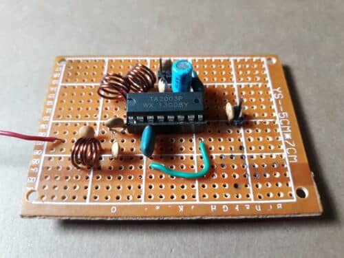
Right here is an easy FM Radio Receiver Utilizing single chip TA 2003. This IC have inbuilt RF Amplifier, native oscillator, a mixer, FM detector and AF preamplifier. Solely few passive elements like ceramic capacitors, X1, X2 each are 10.7MHz 3-pin, 2-pin, do-it-yourself inductors like L1, L2 and L3,an electrolytic capacitor 2.2uF/25V are used on this circuit. 10.7 MHz IFT coil just isn’t used right here so there isn’t a must tune of coils.
Components Record
| Semiconductors IC1: TA 2003 Ceramic capacitors Electrolytic Capacitor Ceramic Filter Miscellaneous |
Circuit Description
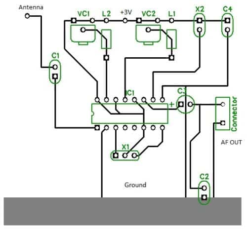
Pin 1 of IC1 TA 2003 is related to antenna (75cm lengthy wire) by means of C1. A capacitor C3 is c. Pin 2, pin 9 are grounded.
A crystal 10.7 MHz 3-pin is related to pin 3 and eight (color tag is confronted in the direction of pin 3) and center pin is related to+3 Vcc.
Pin 13 is related to coil L2 and VC1b in parallel to one another . Different one finish is related to +3 Vcc. Pin 6 and pin 14 are related to +3Volts. A coil L1 and VC1b are related to one another in parallel. One finish of L1 and VC1a is related to pin 15 and others finish is related to +3Vcc. Pin2, 9 are grounded.
Ceramic filter X2 (10.7 MHz 2-pin) is related to +3 Vcc and pin 10. Pin 11 is an output pin and is related to AF amplifier by means of an electrolytic capacitor 10uF/25V. A capacitor C4 is an electrolytic capacitor is of (220uF/25V) related to damaging terminal and +3Vcc which can filter a DC +3Vcc.voltage. And capacitor C2 will filters a noise symbolize at AF output. And an AF output is taken output from pin 11 of IC1 by means of an electrolytic capacitor C3 (10uF/25V).

Development
A veroboard of 5cmX7cm is appropriate to construct your prototype. A PCB format is given within the article is appropriate to construct your prototype.
Now you’ll make coil L1, L2. For a coil L1 a 22SWG wire is wound on 5mm diameter with 3 flip’s air core and coil L2 is 22 SWG wire 5mm diameter wound on 4 turns of air core.
Now insert an 16-pins IC socket on a center of a vero board and solder it. Now take an IC1 TA 2003 and place it on an 8-pin IC socket. Subsequent insert a coil L1, L2 as given in a diagram and in addition X1(3-pins 10.7MHz ceramic filter), and X2 (2-pin 10.7MHz ceramic filter). Chances are you’ll place 2-pin connector for AF output and in addition for +3 V and damaging terminal of+3V battery.
Calibration and Adjustment
For a calibration you want an AF amplifier which is related to output pin 11 of IC1. Take a 2*1.5 Volts battery and join each 1*2 V battery in sequence and hook up with a +3V terminal and floor)
Now flip a quantity of AF amplifier. You’ll hear a snowy as on TV set. Subsequent gently modify coil L1and L2 by pulling them aside Chances are you’ll catch a few of FM stations. Join VC1a and VC2b gang variable capacitor in parallel with L1, L2. Tune a VC1a, b to a strongest station. As quickly as you’ll hear a transparent and loud sound, you could tune to totally different stations.
[ad_2]